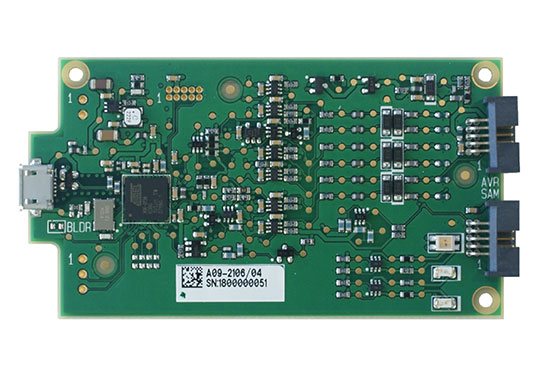
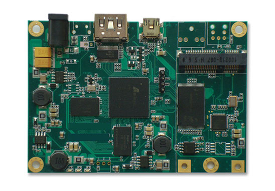
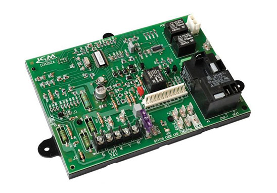
Copper clad is an important part in PCB design. Whether it is domestic PCB design software, or some foreign Protel, PowerPCB (PCB Design Software) provides intelligent copper cladding function, so how to do good copper clad?

What is copper clad?
The so-called copper clad is to use the spare space on the PCB as the reference plane, and then fill it with solid copper. These copper areas are also called copper pouring. The significance of copper clad: 1.Reduce the impedance of the ground wire; 2.Improve the anti-interference ability; 3.Reduce the voltage drop; 4.Improve the power efficiency; 5.Connect to the ground wire; 6.Reduce the loop area.
Precautions for copper clad in PCB design
1. If there are many grounds on the PCB, such as SGND, AGND, GND, etc., At this time, according to the different positions of the PCB surface, the most important “ground” is used as the reference to independently copper clad, and the digital ground and the analog ground are separated. There is not much to say about copper clad. At the same time, before copper clad, first thicken the corresponding power supply lines: 5.0V, 3.3V, etc. In this way, multiple deformable structures of different shapes are formed.
2. For single-point connection of different grounds, the method is to connect through 0 ohm resistance or magnetic beads or inductance;
3. The copper clad near the crystal oscillator, the crystal oscillator in the circuit is a high-frequency emission source, the method is to wrap copper around the crystal oscillator, and then ground the shell of the crystal oscillator separately.
4. The island (dead zone) problem, if you think it is too big, then it doesn’t take much to define a ground via and add it.
5. At the beginning of routing, the ground wire should be treated equally, and the ground trace should be routed well when routing. It is not possible to eliminate the ground pins that are connected by adding vias after copper clad. This effect is very bad.
6. It is best not to have sharp corners on the PCB board (<=180 degrees), because from the electromagnetic point of view, this constitutes a transmitting antenna. For others that will always have an effect just big or small, I recommend using the edge of the arc.
7. Do not apply copper in the open area of the trace in the middle layer of the multi-layer board. Because it’s hard for you to make this copper “good ground”
8. Metals inside the device, such as metal heat sinks, metal reinforcement bars, etc., must be “well grounded”.
9. The heat dissipation metal block of the three-terminal voltage stabilizer must be well grounded. The ground isolation belt near the crystal oscillator must be well grounded.
In a word, if the grounding problem of the copper on the PCB is dealt with, it will definitely be “pros outweigh the cons”. It can reduce the return area of the signal line and reduce the electromagnetic interference of the signal to the outside.

Grande Electronics PCB Design Capability
Maximum signal design rate: 10Gbps CML differential signal;
Maximum PCB design layers: 40 layers;
Minimum trace width: 2.4mil;
Minimum trace spacing: 2.4mil;
Minimum BGA PIN spacing: 0.4mm;
Minimum mechanical hole diameter: 6mil;
Minimum laser drilling diameter: 4mil;
Maximum number of PINs: ;63000+
Maximum number of components: 3600;
Maximum number of BGAs: 48+.

