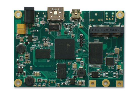
Mark points, also called datum points, provide a common position-able circuit pattern for all steps in the SMT assembly process. mark points are critical to SMT processing and production, next Grande will introduces you to the mark point design specifications for PCB design.

MARK point role and categories
MARK point classification.
1, Single board MARK, its role on a single board to locate the location of all circuit features, essential.
2, Panel board MARK, its role on the patchwork board to assist in locating all circuit features, auxiliary positioning.
3, Local MARK, its role is to locate the reference point mark of single component, in order to improve the placement accuracy (QFP, CSP, BGA and other important components must have local MARK), essential.
The MARK point design specifications
All SMT boards must have Mark points, and the relevant SPEC of Mark points are as follows.
1、Shape: Mark point marker is required to be solid circle.
2、Composition: A complete MARK point includes: marker point (or feature point) and open area.
Location
Mark points are located on the circuit board or combination board diagonal relative position and as far as possible distance apart. Preferably distributed in the longest diagonal position.
In order to guarantee the requirement of placement accuracy, SMT requires: in SMT trial run of all machine types (including derivative machine types), each 1pcs PCB board must have at least one pair of MARK point which can be identified by SMT machine in accordance with the design requirement, that is, there must be single MARK. splice board MARK or combination MARK only plays the role of auxiliary positioning.
When assembling the board, the relative position of the MARK points of each single board must be the same. The position of the MARK point on any single board cannot be moved for any reason, resulting in an asymmetric position of the MARK point on each single board.
All the MARK points on the PCB board can only be valid if they meet the following criteria: two MARKs are on the same diagonal and appear in pairs. Therefore, MARK points must appear in pairs before they can be used.
Dimensions
The smallest diameter of a Mark point marker is 1.0 mm [0.040″] and the largest diameter is 3.0 mm [0.120″]. Mark point markers must not vary in size by more than 25 µm [0.001″] on the same printed board.
Special emphasis: the size of all Mark dots on the same board number PCB must be the same (including PCBs of the same board number produced by different manufacturers).
It is recommended that RD-layout unify the Mark point marker diameter of all drawing files to 1.0mm.
Edge distance
Mark point (edge) from the edge of the printed board must be ≥ 5.0mm [0.200″] (machine clamping PCB minimum spacing requirements), and must be in the PCB board rather than on the edge of the board, and to meet the minimum Mark point openness requirements. Emphasis: referred to as MARK point edge distance from the board edge ≥ 5.0mm [0.200″], rather than the center of the MARK point.
Empty degree requirement
Around the Mark point marker, there must be an open area without other circuit features or markers. Open area circle radius r ≥ 2R, R is the radius of the MARK point, r to 3R, machine recognition effect is better. Often found MARK point open area for the character layer blocked or cut by the V-CUT, resulting in SMT machine can not be identified.
Material
Mark point markers can be bare copper, clear oxidation-protected bare copper, nickel or tin plated, or solder coated. If using solder mask ,it should not cover the Mark point or its open area.
Flatness
The surface flatness of the marker should be within 15 microns [0.0006″].
Contrast
The best performance is achieved when there is a high contrast between the Mark dot mark and the substrate material of the printed board.
For all Mark dots the inner background must be the same.
