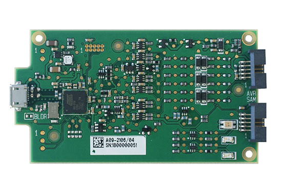
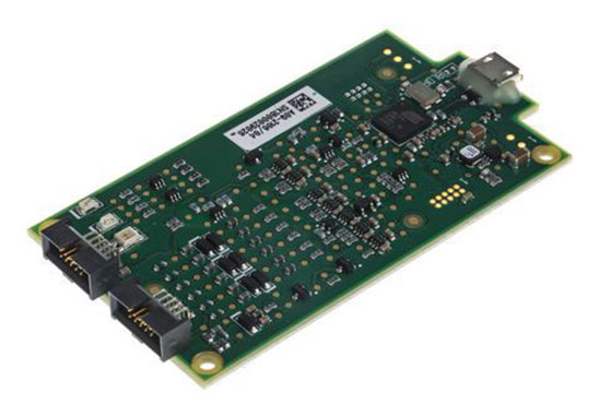
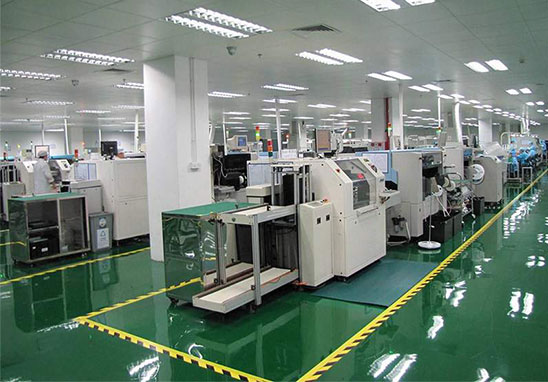
With the miniaturization of electronic equipment, the use of thin PCB printed circuit boards and small components is becoming more and more popular. However, the use of circuit boards with small SMT Assembly components is not only thin but also mostly multilayer PCBs, which apparently also brings some problems. Usually, this kind of PCB will warp during the smt assembly process, and may eventually affect its yield. In addition, excessive warpage will also affect the quality of solder paste printing. Warpage also affects the formation of solder joints during reflow soldering.

What is PCB Assembly Warpage
In PCBA SMT Assembly, the circuit board is prone to warping during reflow soldering. In severe cases, it may even cause defects such as empty soldering of components and tombstones. The causes of PCB board warpage may be different, but in the end it should all be attributed to the fact that the stress applied to the PCB board is greater than the stress that the board material can withstand. When the ability to resist stress is uneven, the result of PCB board warping will appear.
Where does the stress on the board come from? In fact, the biggest source of stress in the reflow soldering process is [temperature]. Temperature will not only make the circuit board soft, but also distort the circuit board, plus the coefficient of thermal expansion (CTE) factor and the material characteristics of [thermal expansion and contraction] , Which forms the warpage of the PCB board.
Causes of PCB Warpage in SMT Assembly
The internal stress on the copper film can cause the circuit board to warp. This is possible even without any heat treatment at room temperature.
In processes involving temperature changes, such as reflow soldering, the difference in thermal expansion coefficient between the copper layer and the substrate can cause warpage.
When individually etched copper clad laminates are stacked together, the difference in the copper density of each layer will cause the stress on each layer to be different, resulting in warpage.
The PCB is usually placed in the panel to improve the efficiency of PCB Assembly. In turn, the paneling uses rails and legs. After assembly, the legs are removed, and the PCB is separated by disassembly. The difference in copper density between the circuit board area and the outrigger area further causes warpage.

SMT Assembly Method To Avoid PCB Warpage
1. Reduce the influence of temperature on board stress
Since [temperature] is the main source of board stress, as long as the temperature of the reflow oven is reduced or the rate of heating and cooling of the board in the reflow oven is slowed, the occurrence of PCB warpage can be greatly reduced. However, other side effects may occur, such as solder short circuit.
2. Using high Tg substrate
Tg is the glass transition temperature, that is, the temperature at which the material changes from the glass state to the rubber state. The lower the Tg value of the material, the faster the board starts to soften after entering the reflow furnace, and the time it takes to become soft rubber state It will also become longer, and the deformation of the board will of course be more serious. The use of a higher Tg sheet can increase its ability to withstand stress and deformation, but the price of the material is relatively high.
3. Increase the thickness of the circuit board
In order to achieve the purpose of lighter and thinner for many electronic products, the thickness of the board has been left 1.0mm, 0.8mm, or even 0.6mm. Such a thickness must keep the board from deforming after the reflow furnace, which is really difficult. It is recommended that if there is no requirement for lightness and thinness, the thickness of the board should be 1.6mm, which can greatly reduce the risk of warpage and deformation of the PCB board.
4. Reduce the size of the circuit board and reduce the number of puzzles
Since most of the reflow furnaces use chains to drive the circuit board forward, the larger the size of the circuit board will be due to its own weight, dent and deformation in the reflow furnace, so try to put the long side of the circuit board as the edge of the board. On the chain of the reflow furnace, the depression and deformation caused by the weight of the circuit board can be reduced. The reduction in the number of panels is also based on this reason. That is to say, when passing the furnace, try to use the narrow edge to pass the furnace direction as far as possible. The amount of depression deformation.
5. Used furnace tray fixture
If the above methods are difficult to achieve, the last is to use the oven tray (reflow solder carrier/template) to reduce the deformation of the circuit board. The principle of the oven tray jig can reduce the warpage of the PCB board is because the jig material is general Aluminum alloy or synthetic stone will be used for high temperature resistance, so the circuit board will undergo high-temperature thermal expansion in the reflow furnace and cold shrinkage after cooling down, and the tray can function to stabilize the circuit board. Wait until the temperature of the circuit board is low. After the Tg value starts to recover and harden, the original size can be maintained.
If the single-layer pallet jig cannot reduce the deformation of the circuit board, you must add another cover to clamp the circuit board with the upper and lower pallets, which can greatly reduce the problem of the circuit board deforming through the reflow furnace. . However, the oven trays are quite expensive, and manual placement and recycling of the trays are required.
6. Use Router instead of V-Cut’s sub-board
Since V-Cut will destroy the structural strength of the panel between the circuit boards, try not to use the V-Cut sub-board or reduce the depth of the V-Cut.

