What is insufficient BGA solder joints in PCBA?
When it comes to PCBA BGA rework, underfilled solder joints refer to insufficient volume of solder joints. BGA solder joints cannot be reliably connected in BGA soldering. The characteristic of underfilled solder joints is that the appearance of the solder joints is obvious during AXI inspection. Smaller than other solder joints.

Reasons
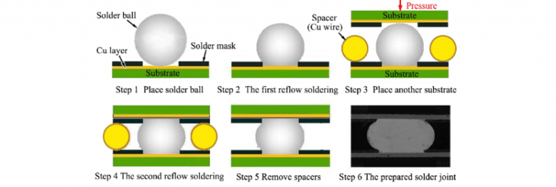
Regarding such BGA problem, the root cause is insufficient solder paste. Another common cause of insufficient solder joints encountered in PCBA BGA rework is the wicking phenomenon of the solder. BGA solder flows into the through hole due to the capillary effect to form information. SMD deviation or printed tin deviation and BGA pads and betrayal vias without solder mask isolation may cause wicking, resulting in insufficient BGA solder joints. Special attention should be paid to the fact that if the solder mask is damaged during the rework process of BGA devices, the wicking phenomenon will be aggravated, leading to the formation of underfilled solder joints.
Incorrect PCB design can also lead to insufficient solder joints. If a hole in the disk is designed on the BGA pad, a large part of the solder will flow into the hole. If the amount of solder paste provided at this time is insufficient, a low Standoff solder joint will be formed. The way to make up is to increase the amount of solder paste printed. When designing the stencil, consider the amount of solder paste absorbed by the holes in the plate, and increase the thickness of the stencil or increase the opening size of the stencil to ensure sufficient solder paste; One solution is to use micro-via technology to replace the hole in the disk design, thereby reducing the loss of solder.
Another factor that produces underfilled solder joints is the poor coplanarity between the device and the PCB. If the amount of solder paste printing is sufficient. However, the gap between BGA and PCB is inconsistent, that is, poor coplanarity will cause insufficient solder joints. This situation is especially common in BGA.

Solution
1)Print enough solder paste;
2)Cover the vias with solder mask to avoid solder loss;
3)Avoid damaging the solder mask during the rework stage of PCBA BGA;
4)Accurate alignment when printing solder paste;
5)Ensureaccuracy ofBGA placement;
6)Operate BGA components correctly during the repair phase;
7)Meet the coplanarity requirements of PCB and BGA to avoid warpage. For example, proper preheating can be adopted in the rework stage;
8)Use micro-hole technology to replace the hole-in-disk design to reduce the loss of solder.

PCBA advantages in Grande
1)Highly professional: Grandefocuses on PCBAsamples, small and medium batches, and promises to deliver goods within 3-5 working days after the materials are confirmed.
2)Professional equipment: Advanced equipment tailored for sample and small and medium batch production, which can paste 0201, BGA pitch 0.3MM, QFN, CSP, CON and other components.
3)Professional technology: 100% of technical backbones have more than 5 years of work experience, and 85% of front-line operators have more than 3 years of work experience.
4)Implements the 5S and 6σ concepts in its daily operations, and has at least 7 checks from incoming materialsto shipment.
5)Promisethat the welding pass-through rate is over 99%. If the customer finds welding defects, repair forfree.

