Do you know what heavy copper PCB is? In this article, we will introduce you to the basic concepts and advanced knowledge of heavy copper printed circuit boards. It is very necessary to read this article before you proceed to import or manufacture heavy copper PCBs. This will make you an expert in the field. Before going into details.

What is PCB?
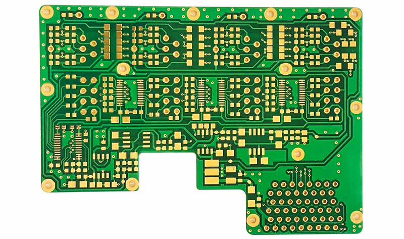
The full name of PCB is Printed Circuit Board. This secures the electrical components on a platform while providing electrical connections and structural support for the components.
Printed circuit boards reduce wiring complexity while increasing circuit reliability. This allows the creation of large circuits and the ability to connect many electronic components with different functions.
In addition, printed circuit boards are free from the complexity of wiring. It does this by connecting components internally through etched conductive paths or lines.
The application of PCB is widely used in various electrical equipment, such as industrial machines, medical equipment, automotive industry, lighting equipment and electrical appliances in different industries.
What is heavy copper PCB?
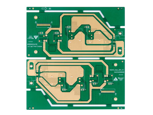
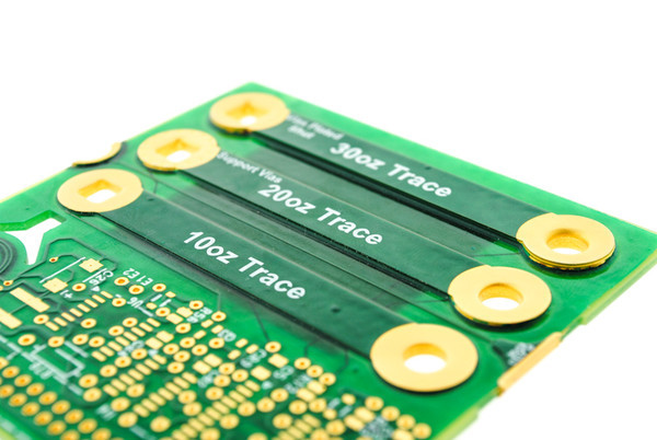
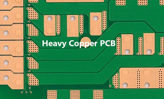
Heavy copper printed circuit boards contain more than three ounces of copper material per square foot and are used to carry high current loads.
You will find copper material thicknesses in the 105 – 400 µm range used in such PCBs. Additionally, heavy copper printed circuit boards are able to maintain dissipation at high temperatures while providing stronger connections.
Additionally, this thermal management feature ensures that the heavy copper PCB is free from thermal stress.

What is the thickness of 5oz copper?
In the printed circuit board industry, one way of expressing the thickness of copper on a printed circuit board is in ounces (oz). Now comes the question – Why use weight units when specifying thickness?
Now, if 1 ounce (about 28.35 grams) of copper were flattened to cover 1 square foot (0.093 square meters) of surface area, the resulting thickness would be 1.37 mils or 0.00348 mm. So for a 5 oz PCB you should expect a thickness of 6.85 mils or 0.1740 mm.

Benefits of using 5oz PCB
Helps conduct large amounts of current
With this feature, heavy copper PCBs can be used in machinery or equipment with high current capability, such as heavy machinery used in industry.
Dissipates heat in an impressive manner
The 5oz PCB is highly efficient in managing thermal energy and ensures the reliability of its performance. They’ll work just fine in high heat, and you won’t find any slack in their performance levels. Furthermore, this feature makes it usable for any high power equipment and machinery.
high mechanical strength
The 5oz PCB provides a strong foundation for its components, making them functionally reliable and robust. This means it provides a great support structure.
It is very compatible with some other materials
During the manufacturing of PCBs, there are other materials that can be used in the manufacturing process. Using different materials can cause compatibility issues that can cause these components to fail. However, with a 5oz PCB, these failures are reduced. This is due to the high compatibility of 5oz PCB with different materials.

Design elements for 5oz PCB
When we’re talking about managing the heat generated in the process, 5 oz PCB can be a very effective option. This happens because 5oz PCB can hold a lot of current and still safely deposit excess heat.
Additionally, you will find that your 5oz design must take into account the need of your application system. So, here are the design elements that you must emphasize.
Spacing of components on a printed circuit board
Dimensions required for the PCB
The type of components you should accommodate on the PCB.
5oz PCB manufacturing process
You can make a 5oz PCB by applying a copper layer on the substrate.
Since copper is known to conduct electricity, you will have a path sufficient to carry current between components.
For applications, you must consider design elements such as component type, spacing, and size before starting the manufacturing process.
There are two main methods in the manufacture of 5oz PCBs.

Etching
This process involves cutting the pattern into a specific surface before highlighting it. In this case, you will pattern the design of the conductive paths on the substrate. This cut pattern is then filled with molten copper.
Plating
This is related to deposits on the surface of the additive material. You also apply this process when making 5 oz PCBs. Here you can deposit copper onto the substrate according to the design of the conductive paths.
Regarding these processes above, you perform them on the substrate. This is achieved through the use of side walls as well as the use of holes for the printed screen.
Design Your 5oz PCB
This can be accomplished using computer-aided software. You will find the software easy to use in both industrial laboratories and academic halls. This allows you to carefully develop the desired PCB design.
The software can be web-based or operating system-based. The software can be used to design circuit diagrams and edit them schematically. Additionally, some software provides simulation capabilities that allow users to export and import the desired functionality into the PCB layout.
Additionally, some allow visualization of 3D designs while allowing all components of the circuit to be incorporated into your design. You can implement all this from anywhere because the software supports different languages.

In Conclusion
You can produce 5oz PCB by electroplating or etching. Such heavy copper PCBs also have different advantages which make them in high demand. Due to its huge advantages and features, the 5oz PCB will surely meet your electrical needs and requirements.
BTW,Grande is a professional PCB manufacturer with more than 20 years of professional experience and leading process capabilities in Rigid PCB, Flex PCB, Rigid-Flex PCB,etc. If you have any PCB/PCBA needs, please feel free to contact us.
